Inspection and Measurement of Solder Cracks and Voids
PCBs and electronic components are becoming smaller and denser, requiring higher quality soldering to mount these components. Analysis of solder defects are especially important for the automotive industry, where advanced computerised control is increasing rapidly.
This section mainly introduces the latest examples of microscopic observation of typical solder defects, such as solder cracks and solder voids, using KEYENCE's latest 4K Digital Microscope.
- Changes in the Environment Surrounding Solder
- Solder Defects and Importance of Observing Solder Cracks and Solder Voids
- Latest Examples of Observation and Analysis of Solder Cracks and Solder Voids
- A Unit Featuring All the Functions Indispensable to Quality Assurance of Solder
Changes in the Environment Surrounding Solder
Smartphones, tablets, and wearable devices continue to be more functional, smaller, and thinner. To make such devices possible, smaller and more layered PCBs have become common.
In the automotive industry, autobraking and autonomous driving require advanced computerised control of the car; because of this, PCBs and other electronic components must be even more durable and reliable.
Solder plays a key role in electric continuity and connection between electronic components and thus is particularly required to have higher durability and reliability. Additionally, the use of lead-free solder, which started in the 2000s, has increased demand for bonding techniques that prevent embrittlement of materials.
Reliability evaluation tests are those tests that are indispensable in the evaluation of the durability and reliability of solder. Among these tests, temperature cycle tests are typically used for evaluating solder.
There are various solder defects that can cause problems. One example is caused by insufficient solder wettability* of solder paste that is automatically applied to a metal plate and printed. Such solder, in concave parts, can decrease bond strength to a solder pad or cause defects such as solder voids. To improve quality, it is essential to use observation and analysis to identify the causes of solder defects. The next section explains typical solder defects, the risks that these defects present, and the necessity of observation.
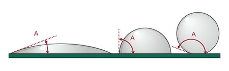
Solder wettability is indicated with a contact angle θ between a solid surface and a liquid (e.g., melted solder) applied to that surface. The smaller that angle A (contact angle θ) in the image is, the higher the solder wettability, indicating a situation where the liquid is widely applied to the solid surface. The larger the contact angle, the lower the solder wettability, indicating a situation where the solid surface repels the applied liquid.
Solder Defects and Importance of Observing Solder Cracks and Solder Voids
Typical solder defects include "solder bridges and "excessive solder" in which too much solder causes short-circuiting. Additionally, "solder splatter" occurs due to excessive heating, while "cold solder joints" occur due to insufficient heating.
There are also “solder cracks” and “solder voids,” which are difficult to detect and identify the causes immediately after mounting. These defects can be caused by various factors and, not only immediately after solder bonds are formed, they can occur or progress over time or due to stress. Therefore, these defects need to be observed and analysed with microscopes or other measuring instruments.
- Causes and risks of solder cracks
- Solder cracks occur or progress due to factors such as fatigue, the passage of time, and the application of stress after solder bonds are formed. If cracks that are microscopic during the initial stages of packaging grow, the resistance of the bond will increase. There are even cases where solder cracks lead to Joule heating. Grown cracks can also completely separate the bond, leading to a component failure. In particular, cracks in lead-free solder are said to progress rapidly once they form. Since grown solder cracks can generate heat and cause fire, they need careful inspection.
- Causes and risks of solder voids
- Solder voids are mainly caused by air bubbles contained in solder that is applied in the printing process of solder reflow, gasses that are generated in the component mounting process, and insufficient solder wettability of solder paste applied to concave parts. Solder voids can decrease solder strength, and partially decreased strength can then cause solder cracks. This is why cause identification of solder voids and countermeasures for such causes are extremely important.
To ensure quality and improve processes, it is important to observe, analyse, and evaluate solder cracks and voids in faulty products.
Latest Examples of Observation and Analysis of Solder Cracks and Solder Voids
Applied solder is three-dimensional, but conventional microscopes only focus on part of it in high-magnification observation due to an insufficient depth of field. Hence, delicate focusing for each part of the observation target is necessary.
Conventional microscopes also do not fully focus on targets having surface irregularities caused by insufficient polishing. Other conventional problems include undetected defects due to reflection from glossy materials and initial subtle cracks that cannot be observed at high magnification or due to insufficient resolution.
KEYENCE’s VHX Series high-definition 4K Digital Microscope can solve these conventional problems, with the high-resolution optical system having a deep depth of field, the 4K CMOS image sensor, and specially designed systems such as high-performance lighting and advanced image processing. More advanced observation, defect analysis, and evaluation of solder can be performed quickly with simple operations, significantly improving work efficiency.
This section introduces the latest examples of observation and analysis of solder defects using the VHX Series.
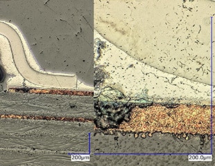
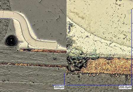
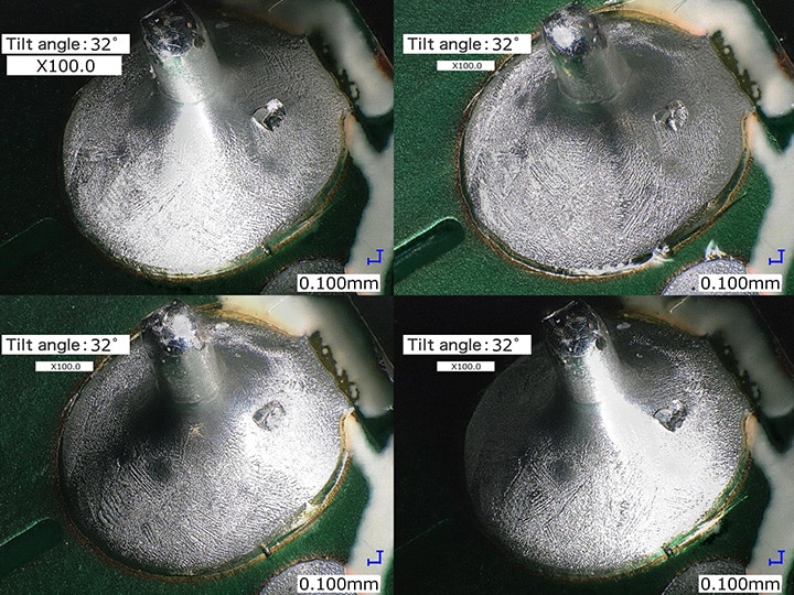
Tilted observation of solder cracks on packaged PCBs
The free-angle observation system of the VHX Series 4K Digital Microscope enables tilted observation of three-dimensional solder fillets on packaged PCBs.
Furthermore, its glare removal function and ring-reflection removal function enable solder crack observations that are both clear and unaffected by solder-specific reflected light.
The VHX Series has achieved a depth of field that is approximately 20 times deeper than that of conventional microscopes. Real-time depth composition is also available and easily creates clear 4K images that fully focus on the entire target, even at high magnification.
Left: depth composition, glare removal, ring-reflection removal/right: normal

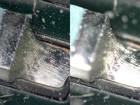
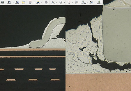
Observation of solder cracks on cross sections of electronic components
Solder cracks that are initially microscopic can grow over time, leading to component failures, heat generation, and fire. Overlooking fine cracks due to insufficient magnification or resolution has been a serious issue.
The high-resolution HR lens and motorised revolver of the VHX Series 4K Digital Microscope enable a seamless zoom function that automatically switches lenses from 20x to 6000x magnification with intuitive operations. A high-magnification image of a defective area can be displayed next to a low-magnification image using the split screen function, allowing users to always track what they are viewing during high-magnification observation.
Furthermore, with a deep depth of field and real-time depth composition, submicron cracks can be observed with a clear image, even if there are surface irregularities.
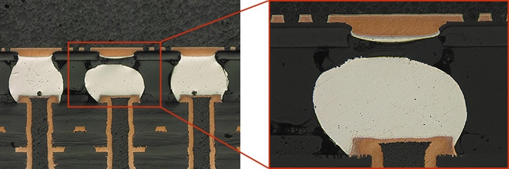
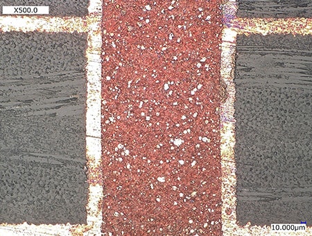
Observation of solder voids on cross section samples
The VHX Series 4K Digital Microscope provides fully focused images of cross-sections, even if there are irregularities introduced by insufficient polishing. These images enable high-resolution observation without any voids being overlooked.
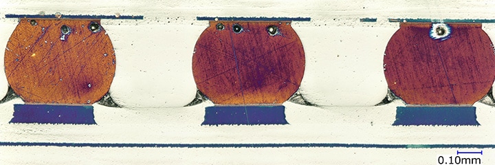
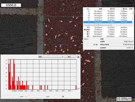
Quantitative analysis of PCB cross sections
The VHX Series 4K Digital Microscope enables high-accuracy automatic area measurement and counting with a high-resolution magnified image. These functions allow users to perform quantitative analysis and generate reports with a single unit, significantly improving efficiency.
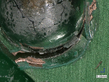
Evaluation of bond strength based on solder fillet appearance
With conventional microscopes, lighting is difficult to set due to the reflection from solder surfaces, causing variations in results among operators.
With the multi-lighting function of the VHX Series 4K Digital Microscope, omnidirectional lighting data is automatically captured with the push of a button.
The most suitable image to use in observation and evaluation can be selected from among the images captured with the multi-lighting function, thereby significantly reducing the time conventionally required for light adjustment. Image data with different lighting is automatically saved, so other images with different lighting conditions can be loaded immediately.
Furthermore, using the glare removal function and ring-reflection removal function suppresses solder-specific reflected light, enabling observations of solder joint appearances with a clear image.
A Unit Featuring All the Functions Indispensable to Quality Assurance of Solder
The VHX Series 4K Digital Microscope has many other functions, such as 2D and 3D measurements, and enables observation, analysis, measurement, and reporting to be performed with a single unit.
For additional product info or inquiries, click the buttons below.
